We are quick and our products are the highest quality.
You don’t need to waste your ti,e getting a quote.
You don’t have to wait a long time to receive your PCBs.
Why spend so much money getting PCBs?
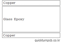
Design Rules 2-10 layers
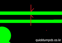
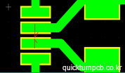
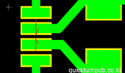
Circuit lines
| Copper thickness (before copper platting) |
Circuit width | Space | Advanced |
|---|---|---|---|
| 0.5 oz(0.018mm) | 3 mil(0.076mm) | 4 mil (0.10mm) | 0.5pitch |
| 1 oz (0.035mm) | 5 mil(0.127mm) | 5 mil(0.127mm) | BGA 3mil(0.075mm) |
| 2 oz (0.070mm) | 6 mil(0.15mm) | 6 mil(0.15mm) |  |
 |
 |
 |
|
| Distance-NPTH : 12mil(0.30mm) | |||
 |
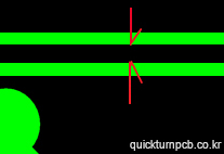
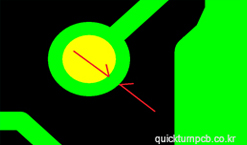
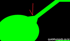
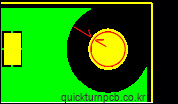
Annular ring
| PTH(via holes) | PTH(components holes) | Recomendation at outer layers & inner layers |
|---|---|---|
| Min. 8mil(0.20mm) | Min. 6mil( 0.15mm) | Teardrop |
 |
 |
 |
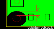
| Via size/pad size | PTH size/pad size | |
| 8mil(0.20mm) drill size/16mil(0.40mm)pad size | 20mil(0.50mm drill size/ 36mil(0.90mm)pad size |
|
| 10mil(0.25mm drill size/20mil(0.50mm)pad size |
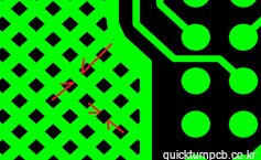
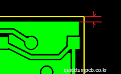
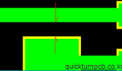
Cross Hatch & Ground plane to outline
| Cross Hatch | Solid plane to outline |
|---|---|
| Min. 10mil(0.25mm) | Min 12mil(0.30mm) |
 |
 |
Solder mask clearance
| SM Clearance | Mask to unexposed copper | SM Dam | SM Clearance for NPTH |
|---|---|---|---|
| Min. 2mil(0.05mm) | Min. 2mil(0.05mm) | Min. 4mil(0.10mm) | Min. 8mil(0.20mm) |
 |
 |
 |
 |
Solder mask at Via holes
| OPEN | Tenting | Wet to Wet | Plugging |
|---|---|---|---|
| Copper exposed | Solder mask 20% | Solder mask 70% | Soler mask 100% |
 |
 |
 |
 |
Silkscreen(Marking)
| Height | Width/Space | Letters to SMD |
|---|---|---|
| Min. 24mil(0.60mm) | Min. 4mil(0.10mm) | Min. 2mil(0.05mm) |
 |
 |
 |
Min. Via hole
| Laminate thickness | Min. Via size |
|---|---|
| 0.062"(1.60mm) or less | 8mil( 0.20mm) |
| 0.095"(2.40mm) or less | 16mil(0.40mm) |
| 0.126"(3.20mm) or less | 20mil(0.50mm) |
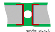
SLOT HOLES(PTH)
| Min. Slot hole width size : 28mil(0.70mm) | |
|---|---|
 |
 |
| OK : Slot hole length size > slot hole width size x 2 + 8mil(0.20mm) |
NG : Slot hole length size < slot hole width size x 2 + 8mil(0.20mm) |
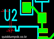
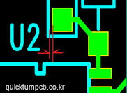
Internal routing
 |
Internal Min. width | PCB thickness |
| 0.062"(1.60mm) Min. 40mil(1.00mm) | ||
| 0.080"-0.125"(2.0mm-2.20mm) Min. 55mil(1.40mm) |
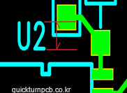
Corner Radius
 |
Min. Radius : R0.127"(0.50mm) |
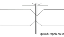
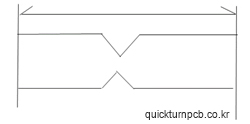
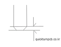
V-cut 1
| PCB thickness | Dim after V-cut | Tol. |
|---|---|---|
| 25mil(0.60mm) | 12mil(0.30mm) | +-4mil(0.10mm) |
| 32mil(0.80mm) | 16mil(0.40mm) | +-4mil(0.10mm) |
| 40mil(1.00mm) | 16mil(0.40mm) | +-4mil(0.10mm) |
| 48mil(1.20mm) | 16mil(0.40mm) | +-4mil(0.10mm) |
| 62mil(1.60mm) | 20mil(0.50mm) | +-4mil(0.10mm) |
| 80mil(2.00mm) | 20mil(0.50mm) | +-4mil(0.10mm) |
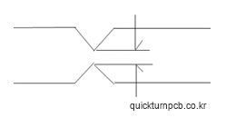
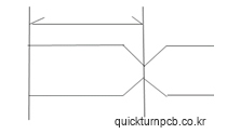
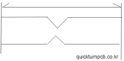
V-cut 2
| Top/Bot Tol. | Size Tol. | Min. Space v-cut center to Circuit |
V-cut angle |
|---|---|---|---|
 |
 |
 |
 |
| + - 8mil(0.20mm) | Min. 20mil(Min. 0.50mm) | 30 degrees |
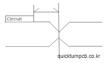
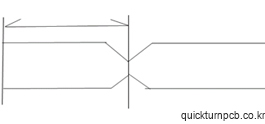
V-cut 3
| Min. board size for V-cut Min. 2.75"(70mm) |
Max. board size for V-cut Max. 18.90"(480mm) |
Min. distance Outline to V-cut center Min. 120mil(3.00mm) |
|---|---|---|
 |
 |
 |
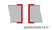
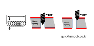
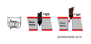
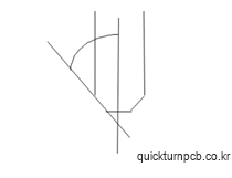
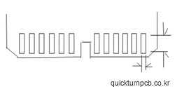
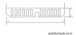
Bevelling for gold fingers
| Good shape for bevelling | Not posssible for bevelling | Bevelling angel 35-45 degrees | Bevelling depth 20mil(0.50mm) |
|---|---|---|---|
 |
 |
 |
 |
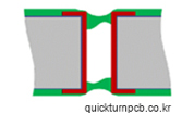
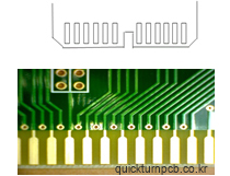
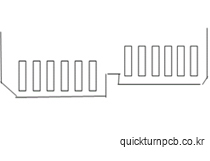
Gold fingers
| Distance each side Min. 5.50"(140mm) |
Standard pin size 40mil(1.00mm)x400mil(10mm) |
Remove solder mask ink at gold fingers zone |
|---|---|---|
 |
 |
 |
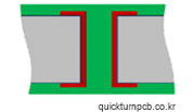
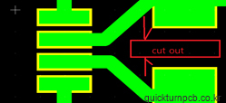
C-cut(half PTH cutting)
| C-cut Min. hole size by routing : Min. 24mil(0.60mm) |
|---|
 |
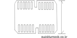
Array distance in a panel
| Internal routing gap : 80mil(2.00mm) Rail bars : 315mil(8.00mm)-400mil(10.00mm) |
|---|
 |
How to Order
- 1 Registration
- 2 Quote & Order
- 3 Upload gerber files
- 4 Payment
- 5 Get your boards on time with high quality
Door to Door Delivery by
UPS, FedEx or DHL


Accept credit cards
in just minutes!
- No Tooling charge
- Free E-test(100%)
- Shipping cost calculated
- High quality
- No MOQ